Third-generation semiconductor GaN and related epitaxial technology brief introduction
1. Third-generation semiconductors
The first-generation semiconductor technology was developed based on semiconductor materials such as Si and Ge. It is the material basis for the development of transistors and integrated circuit technology. The first-generation semiconductor materials laid the foundation for the electronic industry in the 20th century and are the basic materials for integrated circuit technology.
The second-generation semiconductor materials mainly include gallium arsenide, indium phosphide, gallium phosphide, indium arsenide, aluminum arsenide and their ternary compounds. The second-generation semiconductor materials are the foundation of the optoelectronic information industry. On this basis, related industries such as lighting, display, laser, and photovoltaics have been developed. They are widely used in contemporary information technology and optoelectronic display industries.
Representative materials of the third-generation semiconductor materials include gallium nitride and silicon carbide. Due to their wide band gap, high electron saturation drift velocity, high thermal conductivity, and high breakdown field strength, they are ideal materials for preparing high-power density, high-frequency, and low-loss electronic devices. Among them, silicon carbide power devices have the advantages of high energy density, low energy consumption, and small size, and have broad application prospects in new energy vehicles, photovoltaics, rail transportation, big data, and other fields. Gallium nitride RF devices have the advantages of high frequency, high power, wide bandwidth, low power consumption and small size, and have broad application prospects in 5G communications, the Internet of Things, military radar and other fields. In addition, gallium nitride-based power devices have been widely used in the low-voltage field. In addition, in recent years, emerging gallium oxide materials are expected to form technical complementarity with existing SiC and GaN technologies, and have potential application prospects in the low-frequency and high-voltage fields.
Compared with the second-generation semiconductor materials, the third-generation semiconductor materials have wider bandgap width (the bandgap width of Si, a typical material of the first-generation semiconductor material, is about 1.1eV, the bandgap width of GaAs, a typical material of the second-generation semiconductor material, is about 1.42eV, and the bandgap width of GaN, a typical material of the third-generation semiconductor material, is above 2.3eV), stronger radiation resistance, stronger resistance to electric field breakdown, and higher temperature resistance. The third-generation semiconductor materials with wider bandgap width are particularly suitable for the production of radiation-resistant, high-frequency, high-power and high-integration-density electronic devices. Their applications in microwave radio frequency devices, LEDs, lasers, power devices and other fields have attracted much attention, and they have shown broad development prospects in mobile communications, smart grids, rail transit, new energy vehicles, consumer electronics, and ultraviolet and blue-green light devices [1].
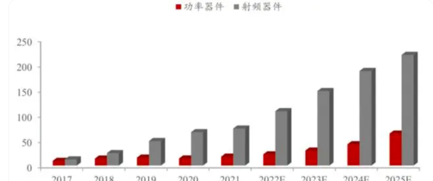
Image source: CASA, Zheshang Securities Research Institute
Figure 1 GaN power device time scale and forecast
II GaN material structure and characteristics
GaN is a direct bandgap semiconductor. The bandgap width of the wurtzite structure at room temperature is about 3.26eV. GaN materials have three main crystal structures, namely wurtzite structure, sphalerite structure and rock salt structure. Among them, the wurtzite structure is the most stable crystal structure. Figure 2 is a diagram of the hexagonal wurtzite structure of GaN. The wurtzite structure of GaN material belongs to a hexagonal close-packed structure. Each unit cell has 12 atoms, including 6 N atoms and 6 Ga atoms. Each Ga (N) atom forms a bond with the 4 nearest N (Ga) atoms and is stacked in the order of ABABAB… along the [0001] direction [2].
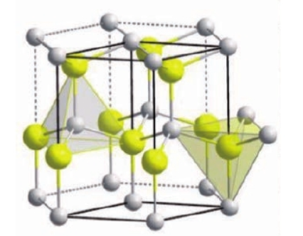
Figure 2 Wurtzite structure GaN crystal cell diagram
III Commonly used substrates for GaN epitaxy
It seems that homogeneous epitaxy on GaN substrates is the best choice for GaN epitaxy. However, due to the large bond energy of GaN, when the temperature reaches the melting point of 2500℃, its corresponding decomposition pressure is about 4.5GPa. When the decomposition pressure is lower than this pressure, GaN does not melt but decomposes directly. This makes mature substrate preparation technologies such as the Czochralski method unsuitable for the preparation of GaN single crystal substrates, making GaN substrates difficult to mass produce and costly. Therefore, the substrates commonly used in GaN epitaxial growth are mainly Si, SiC, sapphire, etc. [3].
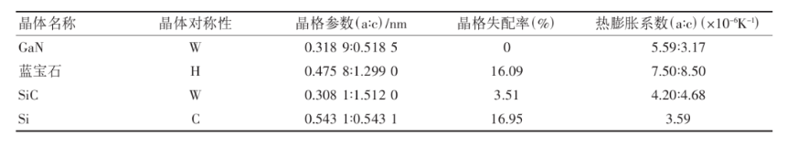
Chart 3 GaN and parameters of commonly used substrate materials
GaN epitaxy on sapphire
Sapphire has stable chemical properties, is cheap, and has a high maturity of large-scale production industry. Therefore, it has become one of the earliest and most widely used substrate materials in semiconductor device engineering. As one of the commonly used substrates for GaN epitaxy, the main problems that need to be solved for sapphire substrates are:
• Due to the large lattice mismatch between sapphire (Al2O3) and GaN (about 15%), the defect density at the interface between the epitaxial layer and the substrate is very high. In order to reduce its adverse effects, the substrate must be subjected to complex pretreatment before the epitaxy process begins. Before growing GaN epitaxy on sapphire substrates, the substrate surface must first be strictly cleaned to remove contaminants, residual polishing damage, etc., and to produce steps and step surface structures. Then, the substrate surface is nitrided to change the wetting properties of the epitaxial layer. Finally, a thin AlN buffer layer (usually 10-100nm thick) needs to be deposited on the substrate surface and annealed at low temperature to prepare for the final epitaxial growth. Even so, the dislocation density in GaN epitaxial films grown on sapphire substrates is still higher than that of homoepitaxial films (about 1010cm-2, compared with essentially zero dislocation density in silicon homoepitaxial films or gallium arsenide homoepitaxial films, or between 102 and 104cm-2). The higher defect density reduces carrier mobility, thereby shortening minority carrier lifetime and reducing thermal conductivity, all of which will reduce device performance [4];
• The thermal expansion coefficient of sapphire is greater than that of GaN, so biaxial compressive stress will be generated in the epitaxial layer during the process of cooling from the deposition temperature to room temperature. For thicker epitaxial films, this stress may cause cracking of the film or even the substrate;
• Compared with other substrates, the thermal conductivity of sapphire substrates is lower (about 0.25W*cm-1*K-1 at 100℃), and the heat dissipation performance is poor;
• Due to its poor conductivity, sapphire substrates are not conducive to their integration and application with other semiconductor devices.
Although the defect density of GaN epitaxial layers grown on sapphire substrates is high, it does not seem to significantly reduce the optoelectronic performance of GaN-based blue-green LEDs, so sapphire substrates are still commonly used substrates for GaN-based LEDs.
With the development of more new applications of GaN devices such as lasers or other high-density power devices, the inherent defects of sapphire substrates have increasingly become a limitation on their application. In addition, with the development of SiC substrate growth technology, cost reduction and the maturity of GaN epitaxial technology on Si substrates, more research on growing GaN epitaxial layers on sapphire substrates has gradually shown a cooling trend.
GaN epitaxy on SiC
Compared with sapphire, SiC substrates (4H- and 6H-crystals) have a smaller lattice mismatch with GaN epitaxial layers (3.1%, equivalent to [0001] oriented epitaxial films), higher thermal conductivity (about 3.8W*cm-1*K-1), etc. In addition, the conductivity of SiC substrates also allows electrical contacts to be made on the back of the substrate, which helps to simplify the device structure. The existence of these advantages has attracted more and more researchers to work on GaN epitaxy on silicon carbide substrates.
However, working directly on SiC substrates to avoid growing GaN epilayers also faces a series of disadvantages, including the following:
• The surface roughness of SiC substrates is much higher than that of sapphire substrates (sapphire roughness 0.1nm RMS, SiC roughness 1nm RMS), SiC substrates have high hardness and poor processing performance, and this roughness and residual polishing damage are also one of the sources of defects in GaN epilayers.
• The screw dislocation density of SiC substrates is high (dislocation density 103-104cm-2), screw dislocations may propagate to the GaN epilayer and reduce device performance;
• The atomic arrangement on the substrate surface induces the formation of stacking faults (BSFs) in the GaN epilayer. For epitaxial GaN on SiC substrates, there are multiple possible atomic arrangement orders on the substrate, resulting in inconsistent initial atomic stacking order of the epitaxial GaN layer on it, which is prone to stacking faults. Stacking faults (SFs) introduce built-in electric fields along the c-axis, leading to problems such as leakage of in-plane carrier separation devices;
• The thermal expansion coefficient of SiC substrate is smaller than that of AlN and GaN, which causes thermal stress accumulation between the epitaxial layer and the substrate during the cooling process. Waltereit and Brand predicted based on their research results that this problem can be alleviated or solved by growing GaN epitaxial layers on thin, coherently strained AlN nucleation layers;
• The problem of poor wettability of Ga atoms. When growing GaN epitaxial layers directly on the SiC surface, due to the poor wettability between the two atoms, GaN is prone to 3D island growth on the substrate surface. Introducing a buffer layer is the most commonly used solution to improve the quality of epitaxial materials in GaN epitaxy. Introducing an AlN or AlxGa1-xN buffer layer can effectively improve the wettability of the SiC surface and make the GaN epitaxial layer grow in two dimensions. In addition, it can also regulate stress and prevent substrate defects from extending to GaN epitaxy;
• The preparation technology of SiC substrates is immature, the substrate cost is high, and there are few suppliers and little supply.
Torres et al.’s research shows that etching the SiC substrate with H2 at high temperature (1600°C) before epitaxy can produce a more ordered step structure on the substrate surface, thereby obtaining a higher quality AlN epitaxial film than when it is directly grown on the original substrate surface. Xie and his team’s research also shows that etching pretreatment of the silicon carbide substrate can significantly improve the surface morphology and crystal quality of the GaN epitaxial layer. Smith et al. found that threading dislocations originating from the substrate/buffer layer and buffer layer/epitaxial layer interfaces are related to the flatness of the substrate [5].
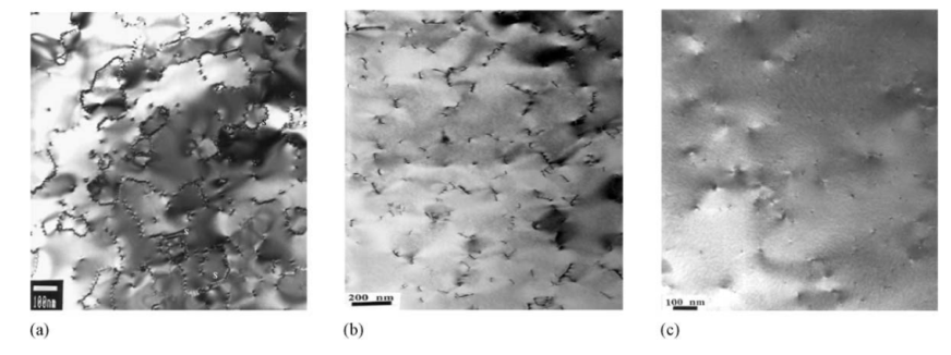
Figure 4 TEM morphology of GaN epitaxial layer samples grown on 6H-SiC substrate (0001) under different surface treatment conditions (a) chemical cleaning; (b) chemical cleaning + hydrogen plasma treatment; (c) chemical cleaning + hydrogen plasma treatment + 1300℃ hydrogen heat treatment for 30min
GaN epitaxy on Si
Compared with silicon carbide, sapphire and other substrates, the silicon substrate preparation process is mature, and it can stably provide mature large-size substrates with high cost performance. At the same time, the thermal conductivity and electrical conductivity are good, and the Si electronic device process is mature. The possibility of perfectly integrating optoelectronic GaN devices with Si electronic devices in the future also makes the growth of GaN epitaxy on silicon very attractive.
However, due to the large difference in lattice constants between Si substrate and GaN material, heterogeneous epitaxy of GaN on Si substrate is a typical large mismatch epitaxy, and it also needs to face a series of problems:
• Surface interface energy problem. When GaN grows on a Si substrate, the surface of the Si substrate will first be nitrided to form an amorphous silicon nitride layer that is not conducive to the nucleation and growth of high-density GaN. In addition, the Si surface will first contact Ga, which will corrode the surface of the Si substrate. At high temperatures, the decomposition of the Si surface will diffuse into the GaN epitaxial layer to form black silicon spots.
• The lattice constant mismatch between GaN and Si is large (~17%), which will lead to the formation of high-density threading dislocations and significantly reduce the quality of the epitaxial layer;
• Compared with Si, GaN has a larger thermal expansion coefficient (GaN’s thermal expansion coefficient is about 5.6×10⁻⁶K-1, Si’s thermal expansion coefficient is about 2.6×10⁻⁶K-1), and cracks may be generated in the GaN epitaxial layer during the cooling of the epitaxial temperature to room temperature;
• Si reacts with NH3 at high temperatures to form polycrystalline SiNx. AlN cannot form a preferentially oriented nucleus on polycrystalline SiNx, which leads to a disordered orientation of the subsequently grown GaN layer and a high number of defects, resulting in poor crystal quality of the GaN epitaxial layer, and even difficulty in forming a single-crystalline GaN epitaxial layer [6].
In order to solve the problem of large lattice mismatch, researchers have tried to introduce materials such as AlAs, GaAs, AlN, GaN, ZnO, and SiC as buffer layers on Si substrates. In order to avoid the formation of polycrystalline SiNx and reduce its adverse effects on the crystal quality of GaN/AlN/Si (111) materials, TMAl is usually required to be introduced for a certain period of time before epitaxial growth of the AlN buffer layer to prevent NH3 from reacting with the exposed Si surface to form SiNx. In addition, epitaxial technologies such as patterned substrate technology can be used to improve the quality of the epitaxial layer. The development of these technologies helps to inhibit the formation of SiNx at the epitaxial interface, promote the two-dimensional growth of the GaN epitaxial layer, and improve the growth quality of the epitaxial layer. In addition, an AlN buffer layer is introduced to compensate for the tensile stress caused by the difference in thermal expansion coefficients to avoid cracks in the GaN epitaxial layer on the silicon substrate. Krost’s research shows that there is a positive correlation between the thickness of the AlN buffer layer and the reduction in strain. When the buffer layer thickness reaches 12nm, an epitaxial layer thicker than 6μm can be grown on a silicon substrate through an appropriate growth scheme without epitaxial layer cracking.
After long-term efforts by researchers, the quality of GaN epitaxial layers grown on silicon substrates has been significantly improved, and devices such as field effect transistors, Schottky barrier ultraviolet detectors, blue-green LEDs and ultraviolet lasers have made significant progress.
In summary, since the commonly used GaN epitaxial substrates are all heterogeneous epitaxy, they all face common problems such as lattice mismatch and large differences in thermal expansion coefficients to varying degrees. Homogeneous epitaxial GaN substrates are limited by the maturity of technology, and the substrates have not yet been mass-produced. The production cost is high, the substrate size is small, and the substrate quality is not ideal. The development of new GaN epitaxial substrates and the improvement of epitaxial quality are still one of the important factors restricting the further development of the GaN epitaxial industry.
IV. Common methods for GaN epitaxy
MOCVD (chemical vapor deposition)
It seems that homogeneous epitaxy on GaN substrates is the best choice for GaN epitaxy. However, since the precursors of chemical vapor deposition are trimethylgallium and ammonia, and the carrier gas is hydrogen, the typical MOCVD growth temperature is about 1000-1100℃, and the growth rate of MOCVD is about a few microns per hour. It can produce steep interfaces at the atomic level, which is very suitable for growing heterojunctions, quantum wells, superlattices and other structures. Its fast growth rate, good uniformity, and suitability for large-area and multi-piece growth are often used in industrial production.MBE (molecular beam epitaxy)In molecular beam epitaxy, Ga uses an elemental source, and active nitrogen is obtained from nitrogen through RF plasma. Compared with the MOCVD method, the MBE growth temperature is about 350-400℃ lower. The lower growth temperature can avoid certain pollution that may be caused by high temperature environments. The MBE system operates under ultra-high vacuum, which allows it to integrate more in-situ detection methods. At the same time, its growth rate and production capacity cannot be compared with MOCVD, and it is more used in scientific research [7].
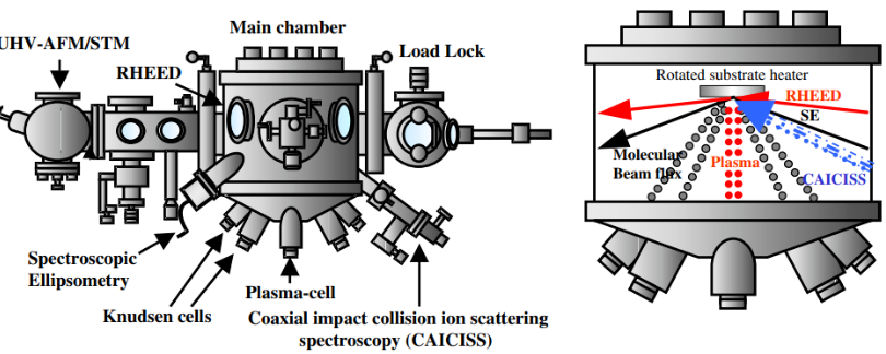
Figure 5 (a) Eiko-MBE schematic (b) MBE main reaction chamber schematic
HVPE method (hydride vapor phase epitaxy)The precursors of the hydride vapor phase epitaxy method are GaCl3 and NH3. Detchprohm et al. used this method to grow a GaN epitaxial layer hundreds of microns thick on the surface of a sapphire substrate. In their experiment, a layer of ZnO was grown between the sapphire substrate and the epitaxial layer as a buffer layer, and the epitaxial layer was peeled off from the substrate surface. Compared with MOCVD and MBE, the main feature of the HVPE method is its high growth rate, which is suitable for the production of thick layers and bulk materials. However, when the thickness of the epitaxial layer exceeds 20μm, the epitaxial layer produced by this method is prone to cracks.Akira USUI introduced patterned substrate technology based on this method. They first grew a thin 1-1.5μm thick GaN epitaxial layer on a sapphire substrate using the MOCVD method. The epitaxial layer consisted of a 20nm thick GaN buffer layer grown under low temperature conditions and a GaN layer grown under high temperature conditions. Then, at 430℃, a layer of SiO2 was plated on the surface of the epitaxial layer, and window stripes were made on the SiO2 film by photolithography. The stripe spacing was 7μm and the mask width ranged from 1μm to 4μm. After this improvement, they obtained a GaN epitaxial layer on a 2-inch diameter sapphire substrate that was crack-free and as smooth as a mirror even when the thickness increased to tens or even hundreds of microns. The defect density was reduced from 109-1010cm-2 of the traditional HVPE method to about 6×107cm-2. They also pointed out in the experiment that when the growth rate exceeded 75μm/h, the sample surface would become rough[8].
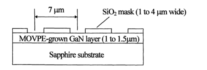
Figure 6 Graphical Substrate Schematic
V. Summary and Outlook
GaN materials began to emerge in 2014 when the blue light LED won the Nobel Prize in Physics that year, and entered the public’s field of fast charging applications in the consumer electronics field. In fact, applications in the power amplifiers and RF devices used in 5G base stations that most people cannot see have also quietly emerged. In recent years, the breakthrough of GaN-based automotive-grade power devices is expected to open up new growth points for the GaN material application market.The huge market demand will surely promote the development of GaN-related industries and technologies. With the maturity and improvement of the GaN-related industrial chain, the problems faced by the current GaN epitaxial technology will eventually be improved or overcome. In the future, people will surely develop more new epitaxial technologies and more excellent substrate options. By then, people will be able to choose the most suitable external research technology and substrate for different application scenarios according to the characteristics of the application scenarios, and produce the most competitive customized products.
Media Contact
Company Name: Ningbo VET Energy Technology Co., Ltd
Email: Send Email
Country: China
Website: https://www.vet-china.com/

